
In 2023, I published a video on my YouTube channel about reading and processing the Behringer UltraNet protocol (see YouTube: Hacking Behringer’s Ultranet for an FPGA-based DIY audio mixer). in this blog post I’d like to take a bit more time to describe the background and the connection between the UltraNet device, FPGA, and the microcontroller so that you can try it by your own.
Table of Contents
- Introduction and background-information about UltraNet
- Audiomixing-functions within the FPGA
- Digital and analog audio output
- Finally, the begin of the Tutorial
- Step 1: Check out GitHub project
- Step 2: Prepare FPGA bitstream
- Step 3: Upload bitstream and test connection
- Step 4: Connect UltraNet device
- Step 5: Signal tests
- Outlook
Introduction and background-information about UltraNet
Ultranet is used by numerous digital audio devices from Behringer, KlarkTeknik, and Midas (all subsidiaries of MusicTribe) to transmit 16 digital audio channels with 24-bit audio and a 48 kHz sampling rate. Well, actually it is a 22-bit audio-connection as the least significant bits are used to address the stereo-pairs, but that’s a topic for the final implementation. UltraNet itself is implemented very nicely in the Powerplay P16-X personal monitoring system (X for numerous sub-devices, like the P16-M Mixer or the P16-I Injector).
I once took a defective P16-I (an analog-to-digital converter for 16 individual channels) and used it to study the protocol, then built a simple digital audio mixer using an Arduino MKR Vidor 4000 board with an FPGA.
This mixer can be controlled via the built-in USB interface as well as via Ethernet (if you add a WIZ5500 chip). What’s particularly nice is that the FPGA makes it very easy to change any functions, resulting in an incredibly flexible DIY audio system that can even output analog signals. How? You can find out either in the YouTube video overview or in detail on the following post. The code and all the necessary design parts are available on my repository on Github.
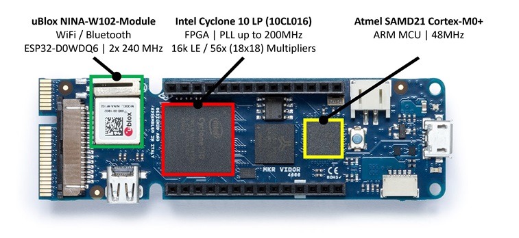
Before we get into the actual topic, I’d like to give you an overview of the toolchain I’ve used: the Arduino board has two independent systems: the SAMD21 microcontroller and the Intel Cyclone 10LP FPGA (see picture above). The microcontroller can be programmed directly in C using the Arduino IDE v2.x in the usual way. The FPGA, on the other hand, cannot be programmed directly with the Arduino toolchain, but requires the free Intel Quartus Prime software from the Intel website. This software allows the synthesis of VHDL and/or Verilog files and enables the interconnection of several individual VHDL blocks via a graphical user interface. After a little familiarization, Quartus is very good for designing digital logic and also for using more complex VHDL blocks from the network.
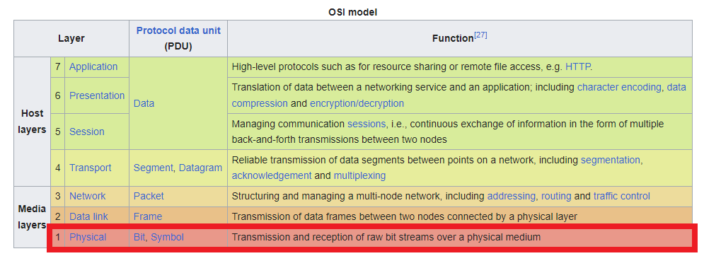
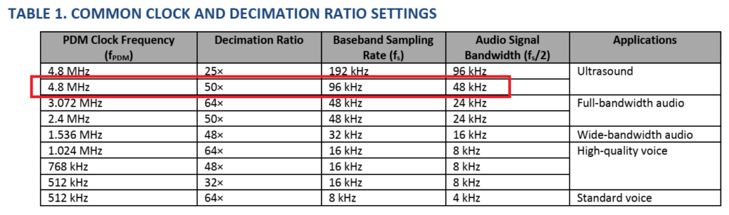
Back to the topic: UltraNet uses a unidirectional data format that was standardized back in 1985: AES/EBU. The AES/EBU standard specifies sample rates for a stereo signal between 32kHz and 192kHz, and bit rates between 16 and 24 bits. Ultranet itself uses 48kHz at 24 bits per channel in this specific case. Since the specification allows up to 192kHz, you get 4 stereo channels transmitted (which means 8 individual audio channels). An ethernet-cable is used as the electrical medium, but only in Layer 1 (physical layer), so that the electrical properties of Ethernet are used, but not the actual Ethernet communication:
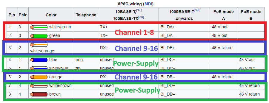
Here, UltraNet uses pins 1/2 for transmitting the audio-channels 1 to 8 and pins 3/6 for audio-channels 9 to 16. Pins 4/5 and 7/8 are intended for supplying a +15V DC voltage to connected devices:
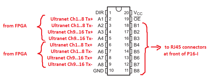
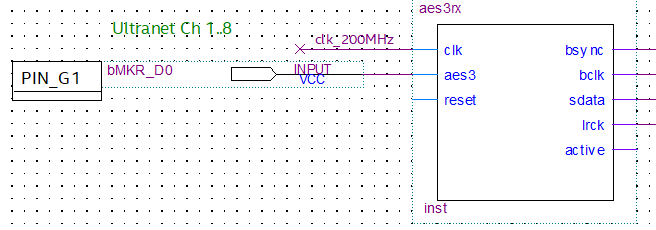
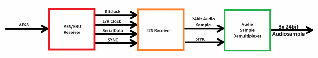
The special thing about AES/EBU is that it does not require return channels and inherently contains a clock rate. This means that two-wire connections or optical connections (TOSLINK) can be used to transmit AES/EBU signals. Due to the higher data rates, it is not really practical to use a microcontroller directly for decoding. However, the Arduino MKR Vidor 4000 has an FPGA on board that can be used to implement digital logic quite well. Petr Nohavica has provided an AES3 receiver block on OpenCores.org that can be used to decode AES3 at various sample rates – have a look at my Code-Section of this website to learn more about receiving AES3-packets in plain VHDL. If this block is clocked at 200 MHz, the 192 kHz Ultranet signal can also be decoded well. In the YouTube video, I simply connected a TX+ input line of the octal buffer IC directly to the Arduino for reception:
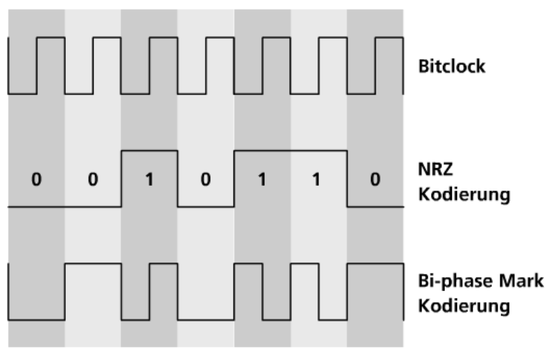
The AES3 receiver then converts the received AES/EBU (UltraNet) signals into a conventional I2S signal. To understand this, we need to take a closer look at the actual AES/EBU format. Since the clock is inherently embedded in the signal, biphase mark encoding is used here, with one exception. The following graphic shows how this signal is generated:
According to a publicly available AppNote, AES/EBU contains the following data:
- 4 bit SYNC-Part (actually this is more than 4 bits, but more down below)
- 20 – 24 bit audio-data
- 4 bit for Parity-bit, Channel-bit, User-Bit and Validation-bit
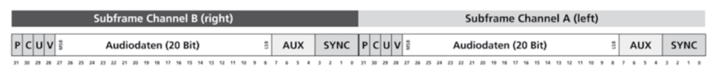
The 4-bit SYNC signal does not actually contain a biphase mark encoded signal, but rather “real” bits, so that we can receive 8 bits here (biphase mark encoding generates a data overhead factor of 2). According to the specification, this SYNC signal has three states: X, Y, and Z (called preamble). All three 8-bit states have a unique pattern that can be used for synchronization. This is exactly what the AES receiver does, outputting the received 24 user data bits (20 audio bits + 4 aux bits) as an I2S signal.
In my approach, these AES-signals are first converted into I2S signals and then into individual 24-bit data vectors in the FPGA. Since the AES/EBU signals are transmitted at 12.288 MHz, the FPGA must decode the signals with a sufficiently high clock rate (200 MHz). I2S is essentially the audio counterpart to I2C (Inter-Integrated Circuit), which is used for communication between ICs. I2S stands for Inter-IC Sound and describes a serial data format in which, in addition to a bit clock, a word clock is used as a synchronization signal and L/R pointers are used alongside the actual data signal. The AES-receiver-block in VHDL only requires a sufficiently high clock (200 MHz in this case) and the input data coming from the P16-I. Then, the output provides the three I2S signals “bit clock” (bclk), “word clock” (lrck), and the serial data (sdata). BSYNC is set to 1 each time a Z preamble is received and marks the reading of channel 1. The “active” output is HIGH when valid UltraNet data is received:
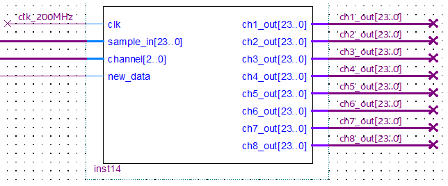
At the output of the block, the audio samples are then available for a brief moment after each valid reception. A reception is signaled with a “HIGH” on the “new_data” output. However, since we want to have access to all 16 channels, I wrote a demultiplexer block that routes the individual audio samples to one of 8 outputs for each new_data matching the channel counter:
From now on, we can do whatever we want with the audio samples we just received. The entire signal chain looks like this:
Audiomixing-functions within the FPGA
What would this whole project be without a basic mixing function? If you add a simple signed integer multiplication to the signal path of the audio samples, you can adjust the volume, since the audio samples basically contain nothing more than the deflection of the speaker dome. So if you lower the level of the individual bits of the audio samples accordingly, the volume is also reduced. To avoid having to calculate fractions, I implemented a simple integer multiplication and ran the volume signal between 0 and 256. I chose 256 because it corresponds to 8 bits:
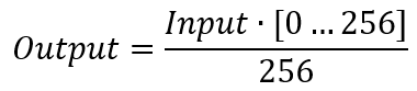
In digital technology (and therefore also in FPGAs), division by 256 can be achieved very easily by shifting the bits 8 bits to the right, which makes the entire calculation very simple. Our volume control is now complete. Downstream from the individual multiplication blocks, I have added two sum blocks that form the audio sum of all connected channels. Here, I am currently using a very simple integer addition, which means that signal clipping can occur if the level of the individual signals is too high:
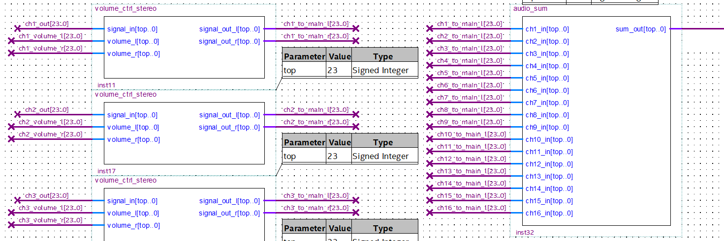
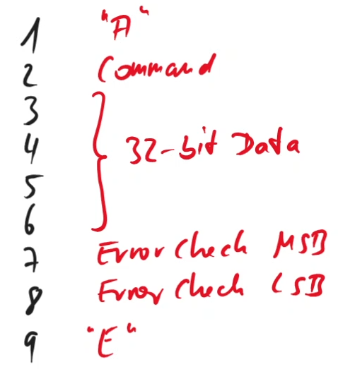
After the two summing blocks, I implemented another volume control to map the two main faders for left and right. But where do the volume signals actually come from? This is where the SAMD21 microcontroller on the board finally comes into play. In the controller’s C code, I implemented a receiver via the serial interface that reads the individual channel values. Alternatively, if a WIZ5500 Ethernet chip is connected, the control can also be set via a terminal interface or, if necessary, a web server. The volume signals are then sent to the FPGA as integer values. Currently, 256 individual volume commands can be transmitted, as I use an 8-bit command to distinguish between the 32-bit user data:
I also used the protocol to implement left/right balancing. The commands are used to set a value for the balance between 0% (far left) and 100% (far right). In the background, however, only the volume for the left and right channels is calculated and then passed on to the FPGA. The microcontroller stores the current absolute volume and balance for each channel and uses this to calculate the necessary volumes for the left and right channels.
Digital and analog audio output
The FPGA can easily output SPDIF signals (AES/EBU) again, allowing you to use a commercially available SPDIF -> analog converter. Once again we can find a nice S/PDIF transmitter block on OpenCores.org: Geir Drange has provided this block. This block expects two of the 16 24-bit vectors and, with a suitable 6.144 MHz clock, can output Biphase Mark Encoded data on a single digital output-pin:
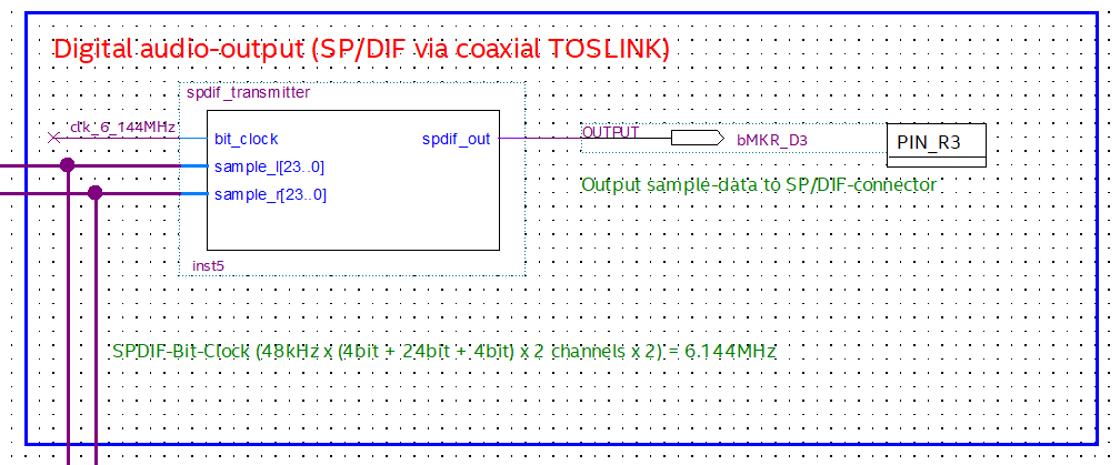
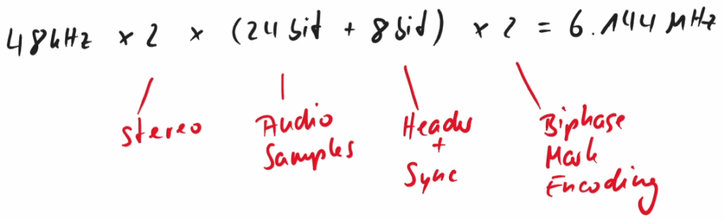
Why exactly 6.144 MHz? Well, due to the Biphase Mark encoding and the bits to be transmitted, we need to get the bits through the line quickly enough:
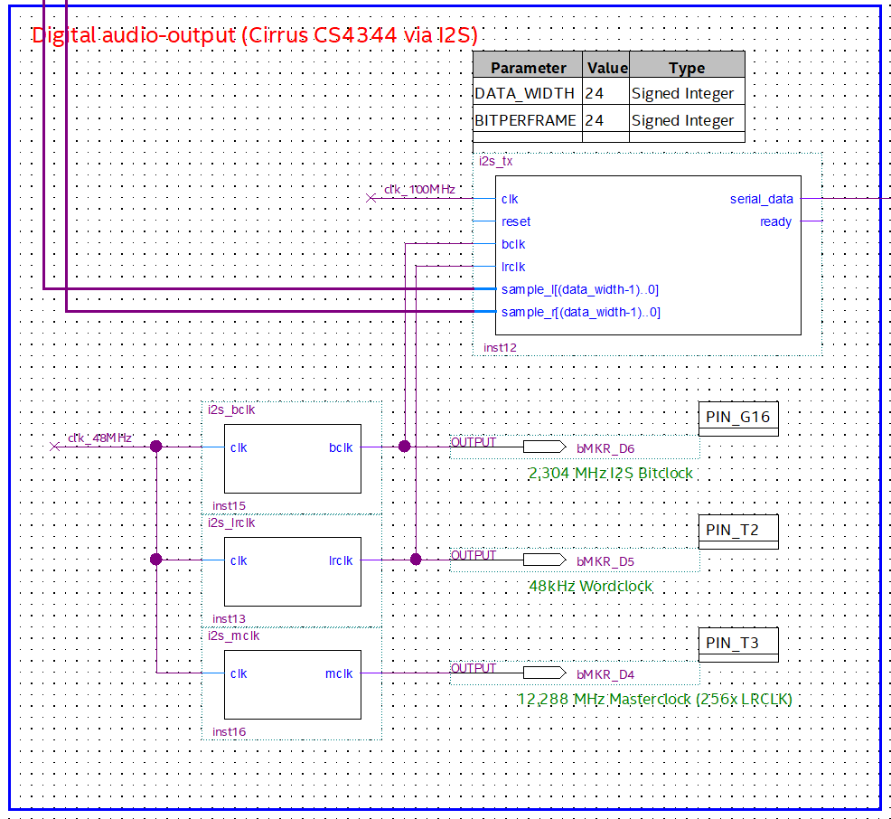
Another option is to simply reuse the audio signals as I2S signals for an external DAC. To do this, the audio samples must be output serially with suitable bit and word clocks:
But what if we want to get analog signals? Well, even a fully digital system is able to output analog data: you just have to switch the digital output on and off fast enough to emulate a corresponding analog signal. For the case of brightness-control of LEDs, PWM (pulse width modulation) is used to adjust it. But for audio signals, a so called pulse density modulation (PDM) is more suitable:
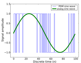
With this method the audio samples can be converted directly and output serially at a digital pin, if the sample rate of the digital pin is sufficiently high. To achieve the intended 48 kHz sample rate, we must set the clock rate of the PDM to at least 2 MHz, better 4.8 MHz:
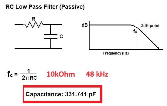
You can then use a simple low-pass filter to convert this digital serial signal into an analog signal with line level, as the FPGA outputs at a voltage of 3.3V:
The resulting audio signal is surprisingly good and more than adequate for everyday tasks. Listening to an MP3 on headphones, I would never have guessed that only a RC-low-pass filter was at work. Audiophiles are probably throwing their hands up in horror right now, but for a general use-case this is sufficient.
Finally, the begin of the Tutorial
In 2023 I’ve stumbled upon this topic rather by accident, and I initially experimented with the Arduino MKR Vidor 4000 board because it was available. That’s how I came across the Intel Cyclone 10LP FPGA, but you can use the logic-blocks described above with a Xilinx/AMD or Lattice FPGA as well. I have continued to use the Arduino MKR Vidor 4000 board as the hardware basis for this tutorial, even by knowing that it is unfortunately marked as “End of Life” by Arduino. Alternatively, you can also use other FPGA boards with Cyclone FPGAs, e.g., the Trenz CYC1000 or comparable boards. The advantage of the Vidor 4000 is simply that, in addition to the FPGA, the board also has an ESP32 and another microcontroller, which can be used to calculate a lot of additional things (e.g., the volume parameters or the EQ settings). However, this is also possible from a PC, so that theoretically the same result can be achieved with the CYC1000.
We need a total of three free tools as software:
- Arduino IDE in version 2.x, download link
- Board support for Arduino SAMD boards (32-bit ARM Cortex-M0+)
- Ticker library by Stefan Staub
- Intel Quartus Prime Lite (e.g., version 24.1), download link
- HTerm, download link
Theoretically, we can work without HTerm, as we can also send the control commands directly from the Windows command line. But it makes the whole thing much easier.
Step 1: Check out GitHub project
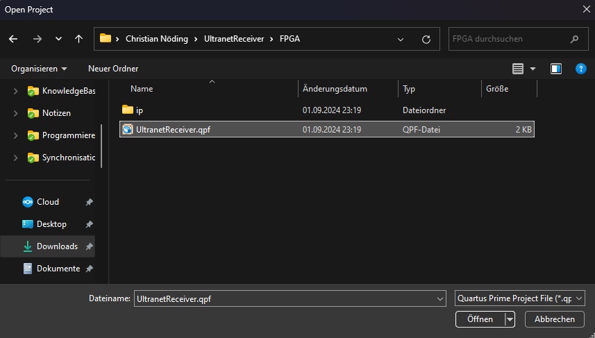
To check out the GitHub project, first install Git from www.git-scm.com. After installing with default settings, start Git Bash either from the Windows Start menu or by pressing Windows+R and then entering “C:\Program Files\Git\git-bash.exe”. With the command “cd ~,” we switch to the home directory of the user account and check out the repository into a new subdirectory with the following command: “git clone https://github.com/xn--nding-jua/UltranetReceiver.git.” We can open the directory with the command Windows+R and then entering “%USERPROFILE%\UltranetReceiver” in Explorer.
Step 2: Prepare FPGA bitstream
Once the basic requirements are met, we start the installed Quartus Prime Lite. All newer versions should work, but let’s take a look at version 25.1. First, we open the Quartus project from the Git repository:
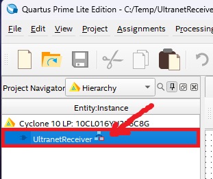
Double-click on the project name on the left-hand side to open the parent schematic:
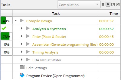
First, we won’t make any adjustments to the logic, so the project just needs to be compiled. Either press CTRL+L or click on “Processing” in the main menu and then on “Start Compilation”:

Depending on your computer, compiling will now take between 2 and 10 minutes:
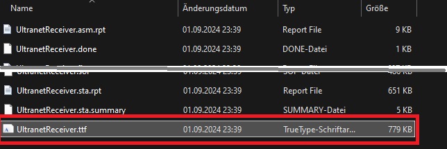
Subsequently, numerous new files will appear in the subdirectory “FPGA\output_files,” including the file that is now important to us: UltranetReceiver.ttf:
Unfortunately, we cannot embed this file directly into our Arduino code yet, but we can convert it into a standard C header file using the included converter tool. To do this, you can either run the batch file “update_fpga_bitstream.bat” from the ‘Controller’ subdirectory or enter the following command directly in the Windows Run dialog: “%USERPROFILE%\UltranetReceiver\Controller\update_fpga_bitstream.bat”. After the short conversion, a new header file “bitstream.h” should have been created in the “Controller” directory:

This completes the FPGA part for now, and we can move on to uploading via the Arduino IDE.
Step 3: Upload bitstream and test connection
From now on, we can do everything via the Arduino IDE in version 2.x. First, start the Arduino IDE. Here, we first need to install support for the SAMD21 and the ESP32. To do this, click on “File,” then on “Preferences…” and then on the blue button on the right-hand side. The following URLs must be entered there:
http://downloads.arduino.cc/Hourly/samd/package_samd-hourly-build_index.json
https://espressif.github.io/arduino-esp32/package_esp32_index.json (<- we don’t need the ESP32 support here, but it’s good preparation for the FPGA audio mixer)
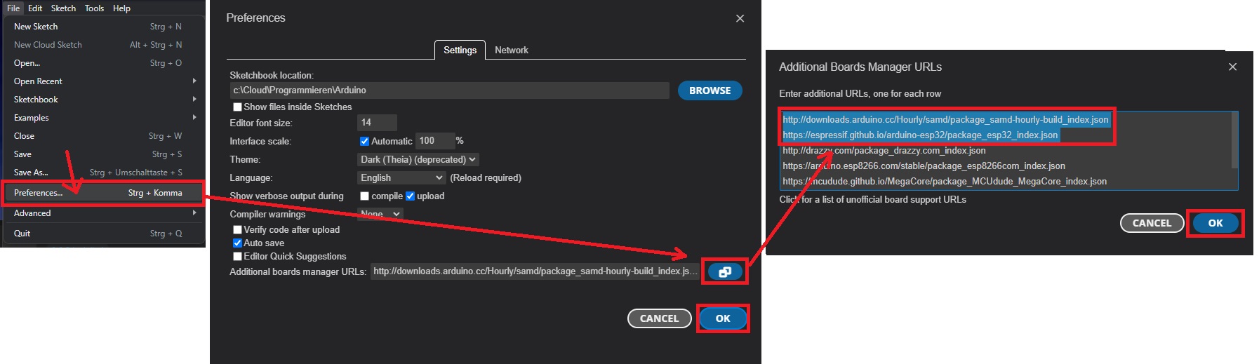
After clicking the OK buttons, you can now search for “samd” in the Boards manager and install support for “Arduino SAMD Boards (32-bits ARM Cortex-M0+).” If you want, you can also install support for the ESP32 at this point (which is included in the NINA W102 of the Vidor 4000). However, this takes a little longer and is not required for this tutorial.
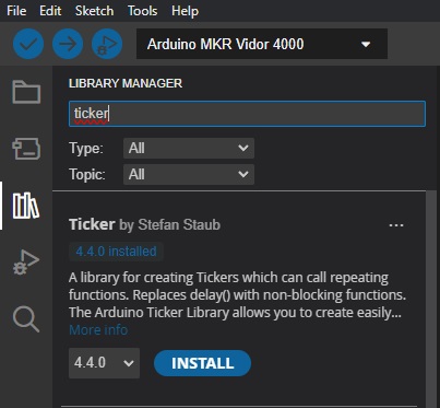
The code now requires an auxiliary library to compile, namely Stefan Staub’s ticker. You can install this library via the Library Manager in the Arduino IDE:
Now is finally a good time to connect the Arduino MKR Vidor 4000 to the USB port. The Arduino IDE should now also find the virtual COM port and display “Arduino MKR Vidor 4000” as the “Board.” You can compile the code by pressing CTRL+R or via the main menu. This should be fairly quick and take only a few seconds. Please don’t be alarmed if you see a few warnings, which are often displayed in red. This is not an error and should look something like this:

Now we are ready to program the SAMD. Press CTRL+U or select “Sketch” from the main menu and then “Upload” to transfer the code to the SAMD21. The SPI flash of the FPGA will also be written with our bitstream, which is why the upload takes a little longer once it reaches about 50%. The board will now reset automatically and the FPGA and SAMD are ready for use.
Note 1: One source of error here is that the Arduino MKR Vidor 4000 demands quite a lot of current. I had major problems with a passive USB hub, and even some notebook USB ports did not work. An active USB hub with a good cable helps a lot here, or connecting directly to a desktop PC.
Note 2: Do not connect the Vidor 4000 directly in the box supplied with the foam. Unfortunately, the black foam is conductive and causes communication problems. Nothing will break, but the Vidor will not boot and the PC will simply display “USB device faulty.”
Now start the downloaded HTerm software and we can perform an initial connection test:
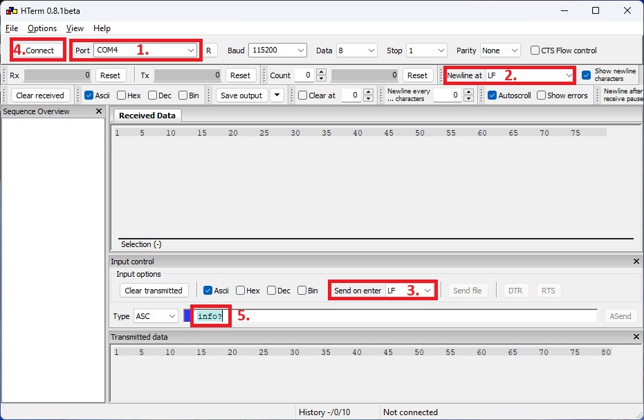
First, select the correct COM port at the top and select “LF” as the end character for both sending and receiving. Now you can establish the connection by clicking on “Connect.” The command “info?” followed by pressing the Enter key or clicking on the ‘ASend’ button on the right should result in the following text appearing in the “Received Data” field:
Ultranet Receiver 0.4.0
FPGA version v0.1
Compiled on 09/02/2024
Info: https://github.com/xn--nding-jua/UltranetReceiverIf nothing happens, please test the COM port and check that the Vidor 4000 is connected correctly – and, above all, that the black foam has been removed from the pins!
Step 4: Connect UltraNet device
If the SAMD sends data back via the COM port, the FPGA will already attempt to decode UltraNet signals. So now we need UltraNet. For my tests, I used a defective P16-I and connected directly to the buffer ICs with jumper wires:
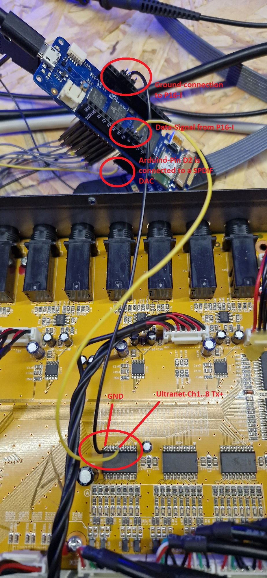
If you don’t want to/can’t do this, you can also use the Tx+ lines of the RJ45 socket. The P16-I apparently continues to transmit the UltraNet signal as a 3.3V signal after the 74LVC245A buffer IC, as this chip can only supply a maximum of 3.65V.
The following pins are currently assigned on the Vidor 4000:
- Pin D0: the FPGA expects Tx of UltraNet channels 1 to 8 here
- Pin D1: the FPGA expects Tx of UltraNet channels 9 to 16 here
- Pin D3: Output of a sum signal as S/PDIF, which can be fed to any standard S/PDIF converter
- Pin D21: Output of a sum signal as PDM, which can be converted back into a proper analog signal using a simple RC filter
- In addition, a regular I2S signal is at D4 to D7:
- Pin D4: I2S MCLK (master clock with 12.288 MHz)
- Pin D5: I2S word clock (48 kHz)
- Pin D6: I2S bit clock (2.304 MHz)
- Pin D7: I2S data (24-bit, 48 kHz, stereo)
For a very simple test, connect an UltraNet stream to pin D0 and either an S/PDIF converter to D3 or an RC low-pass filter to D21. The following is sufficient as an RC:
Step 5: Signal tests
To hear something, we still need to send the volume levels to the FPGA. During initialization, the main volume is set to 100%, but the individual channels are still at 0%. So open HTerm again, select “LF” as the line ending and connect to the correct COM port. If necessary, check the connection again with the command “info?”.
Now you can set the volume to 25% for channel 1, for example. To do this, send the command “vol_ch1@25” or another channel between 1 and 16. The controller should respond with “OK”. In addition, the main volume can be set between 0 and 100 using the commands “vol_main_l@25” and “vol_main_r@25.” A linear volume scaling has been implemented here so far. A logarithmic scaling is available in the second repository “Audiomixer.”
If you cannot hear an audio signal, please check the signal line on D0 and, if necessary, the signal shape with an oscilloscope. In my experience, the slope steepness can be a problem. The signals clock at 12.288 MHz and therefore must not be routed too freely and arbitrarily.
Outlook
So what did this little project achieve? Well, I was able to deepen my knowledge of digital signal processing a little. When I heard about digital technology during my studies 20 years ago, we only covered the basics, but not processing within FPGAs. That’s probably different in today’s studies. Furthermore, you can use this code base to create your own mixing consoles, primarily for processing digital input signals. With this system, you can actually read in several digital signals independently of each other, process them together, and output them again.
If the UltraNet signal is now decoded correctly on your side, have a look at the UltraNet transmitter to send UltraNet by your own, or you may perhaps venture into the next bigger project: the f/bape audio player (f/bape is an acronym for FpgaBaseAudioPlayerwithEqualizer). In addition to the pure audio mixer option, I have implemented EQs, crossovers, audio compressors, and noise gates. Here, the range of functions and possible combinations is limited only by the number of logic elements in the FPGA, and you can definitely build a well-functioning 22-channel digital mixing console with it. So it’s worth taking a look: f/bape – An FPGA-based audio player with equalizer
…and all this with a small Arduino board on a breadboard… I think that’s great 😉