During my time as a scientific researcher at the University of Kassel, I worked on a couple of very different types of laboratory test-devices to check if a theoretical idea is working or not. Most of the time we designed not a very fancy and good looking device, but a functional PCB with the main-components of interest. Here is an excerpt of some nice and hopefully interesting devices with some comments.
Table of Contents
- Construction of a 3kW single-phase inverter for GaN semiconductors and a switching frequency of >400kHz
- Investigating new SiC-semiconductors for high-power converters
- Investigating different types of PV-inverter-topologies
- 3-phase PV-inverter with only 2 HF-switches?
- First contact with power-electronics
- Scientific hardware and software engineering
Construction of a 3kW single-phase inverter for GaN semiconductors and a switching frequency of >400kHz
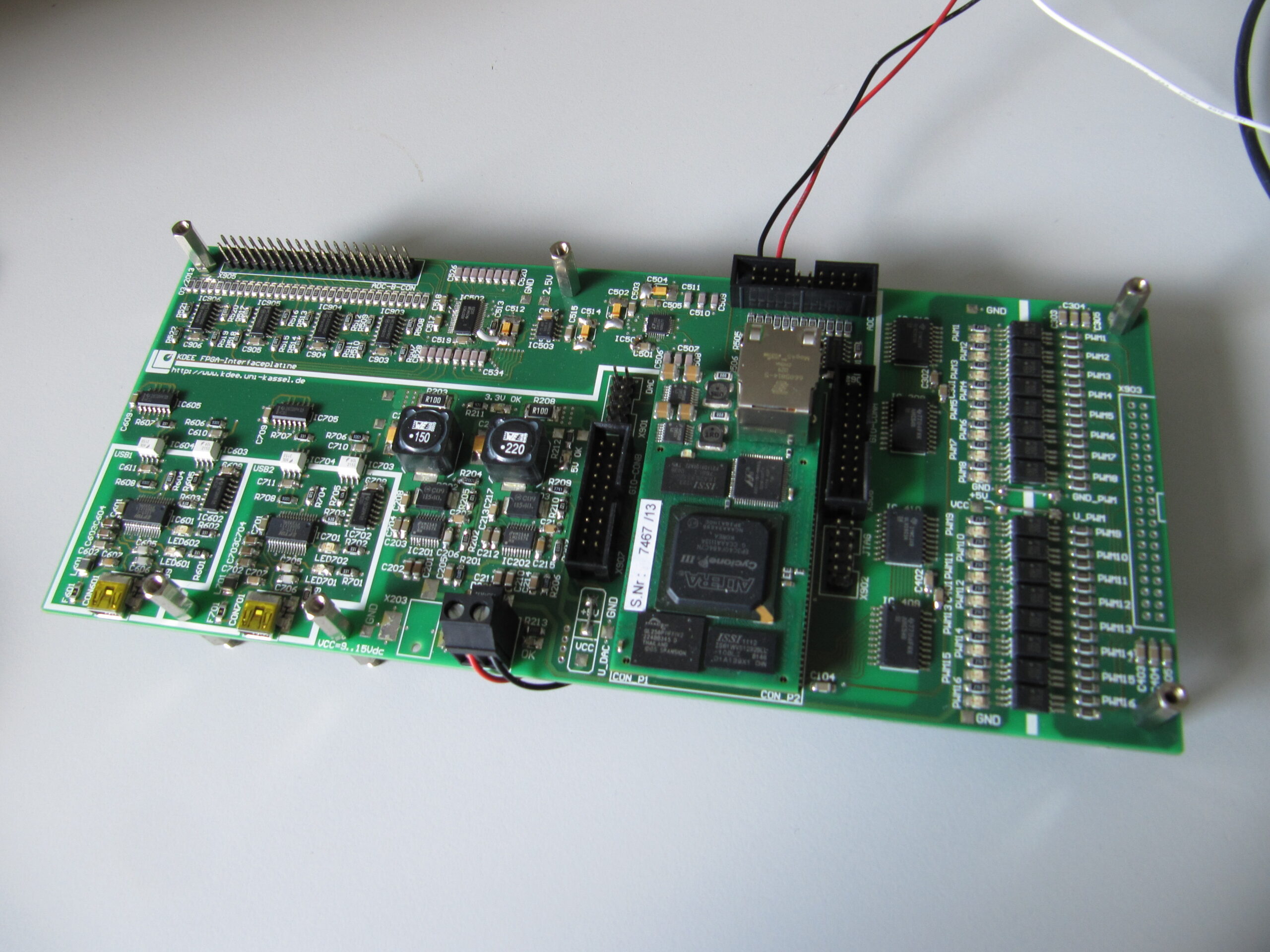
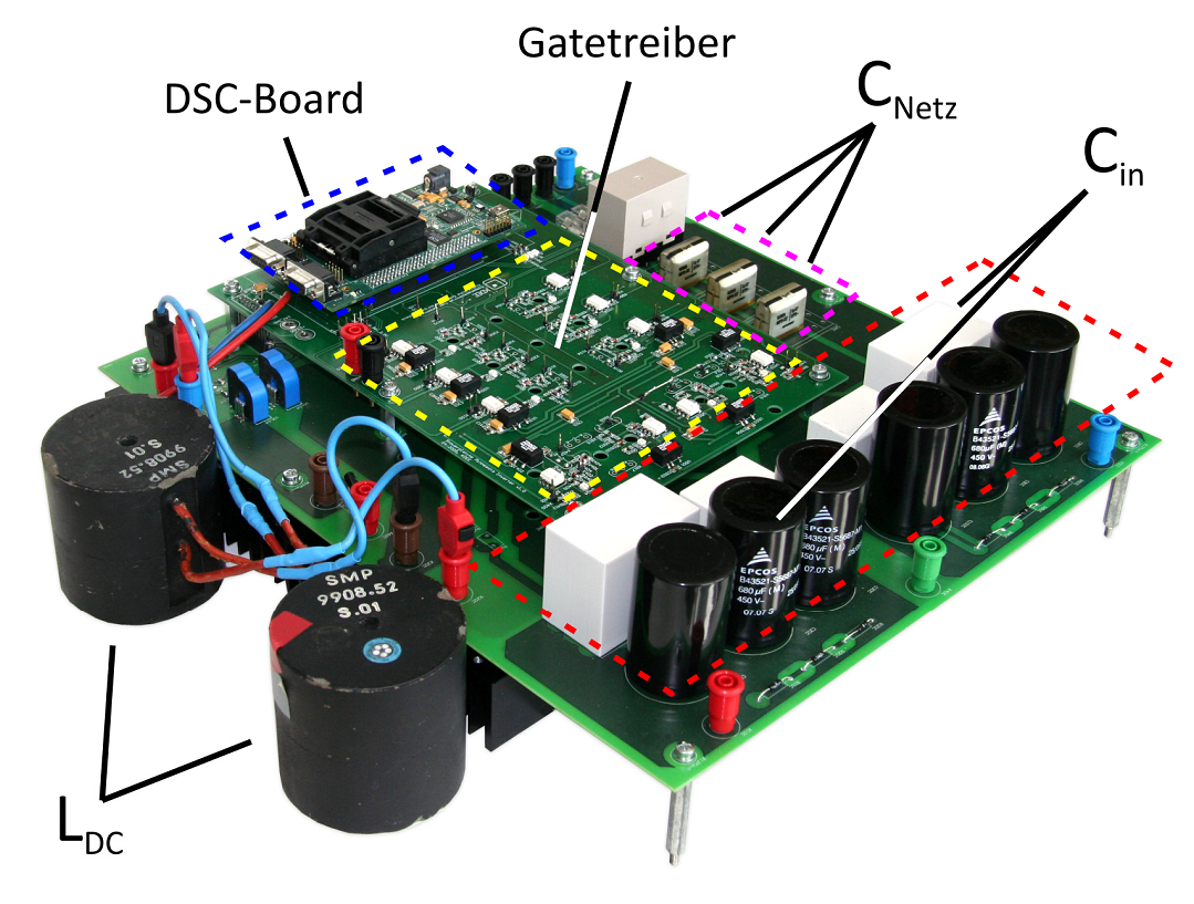
In 2013 we started working on Gallium-Nitrid devices and within the european project E2COGaN (short for “Energy Efficient Conversion using GaN Power Devices”) we designed a 3kW single-phase inverter for GaN semiconductors and a switching frequency of >400kHz. As we were planning to control the current with this high frequency to test the limits of a very low output-filter-inductance, we move from a classical microcontroller-approach to an FPGA-based approach. The available microcontroller was a TI C2000 with 150MHz, but was not able to control a closed-loop current-controller every 2.5µs. So this was the very first contact with FPGAs.
My first task was to design an FPGA-based development board, with ADCs, DACs, multiple PWM-outputs with variable voltages, a powerful supply with a single input-voltage and control-connectors. So I designed a board around the Altera Cyclone III FPGA. For the supply I designed two independent buck-converters that converted a variable input-voltage to 5V and 12V to supply the individual parts of the PCB:
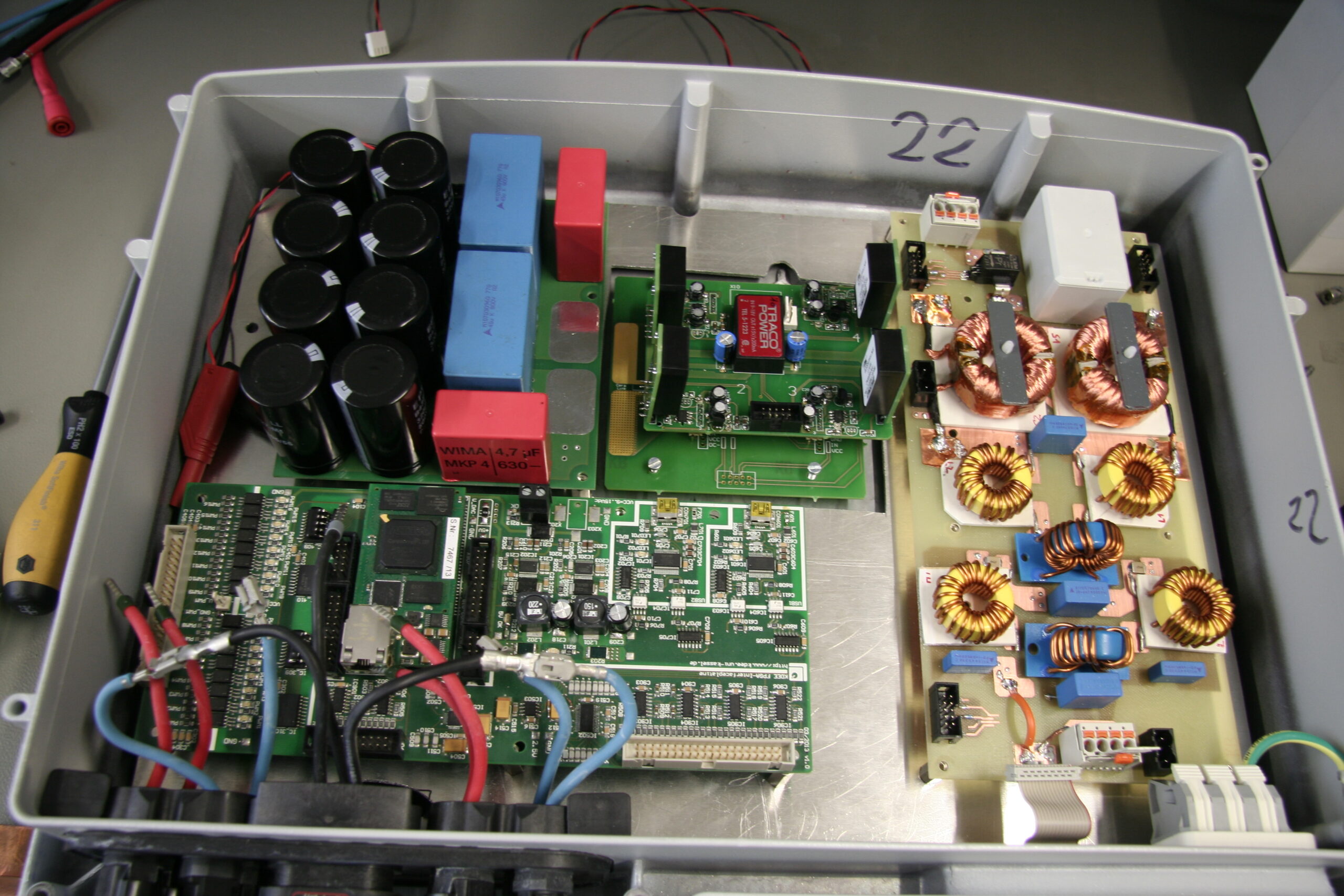
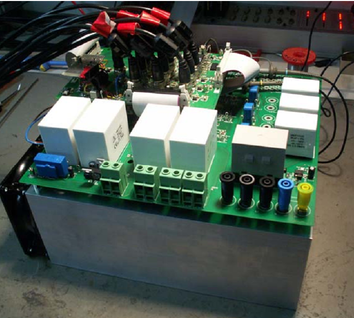
We put the individual PCBs of the first prototype in a housing of an old PV-solar inverter as the heatsink was sufficient for the low losses of the GaN-inverter:
The final prototype was much better looking compared to our laboratory prototype:

If you zoom into the PCB, you might think of a ready-to-market-device 🙂
Investigating new SiC-semiconductors for high-power converters
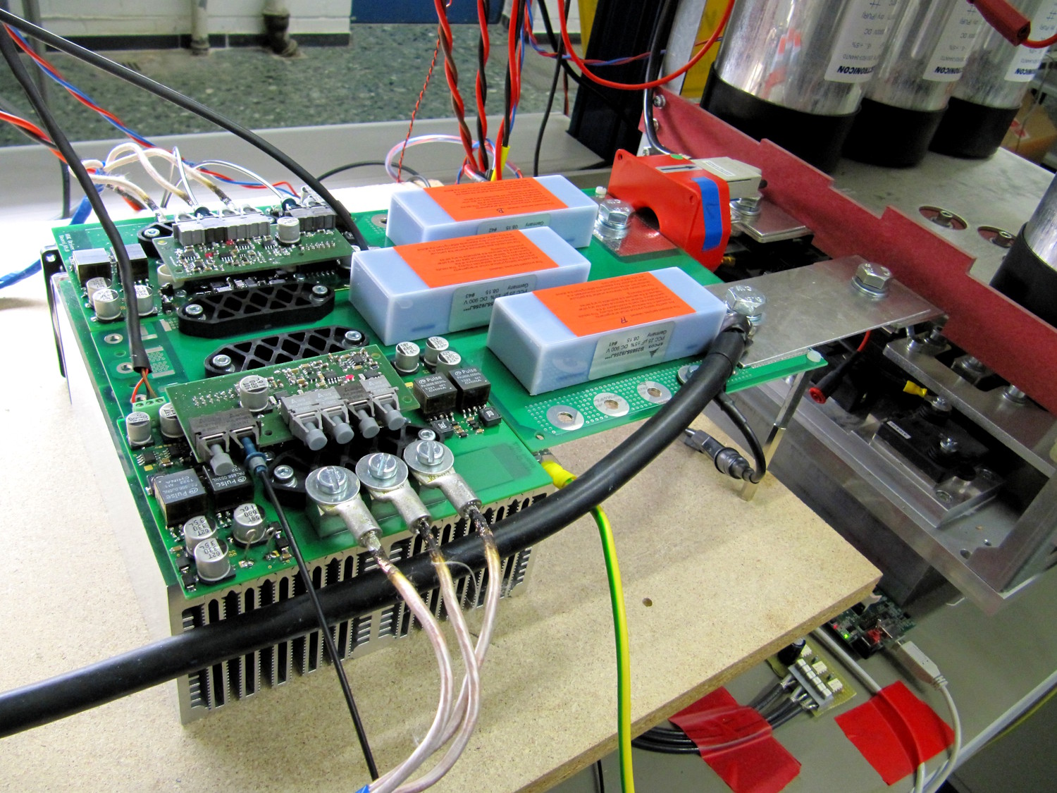
In 2014 I worked together with semiconductor-specialists from Semikron and developer-teams from SMA Solar Technology AG, Siemens Healthcare and TDK Epcos. Semikron developed a new type of SiC-housing that allowed lowest possible parasitic inductances that allowed the SiC-devices to switch with very high dv/dt rates and my task was to investigate the performance within a PV-boost-converter for up to 130kW for utility-scale PV-plants. For this I built up a two-phase interleaved boost-converter that made use of two SiC-MOSFETs. Three special ceramic capacitors made by TDK Epcos supported the lowest-possible parasitic inductance of the SiC device and the PCB:
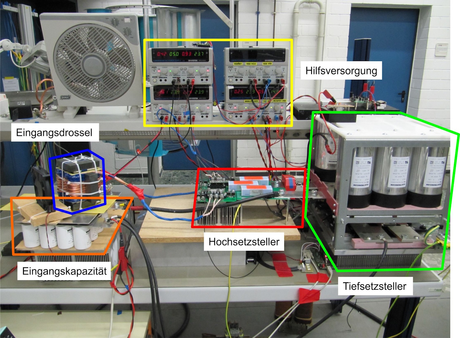
As I was not able to get 130kW out of our grid and had no chance to cool 130kW into the environment, I designed a back-to-back-converter-system. As my device-under-test was a boost-converter, I used an PV-inverter-system as a buck-converter to convert the output-voltage down to a lower value. So only the losses of the system had to be fed by our grid:
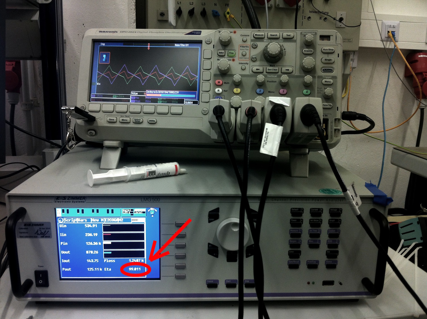
We were quite happy with the results: at 125kW we achieved 99.01% efficiency, resulting in “only” 1.25kW losses:
In the end I was able to achieve the desired 130kW – still with a very good efficiency at this time:

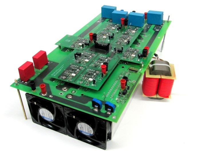
Investigating different types of PV-inverter-topologies
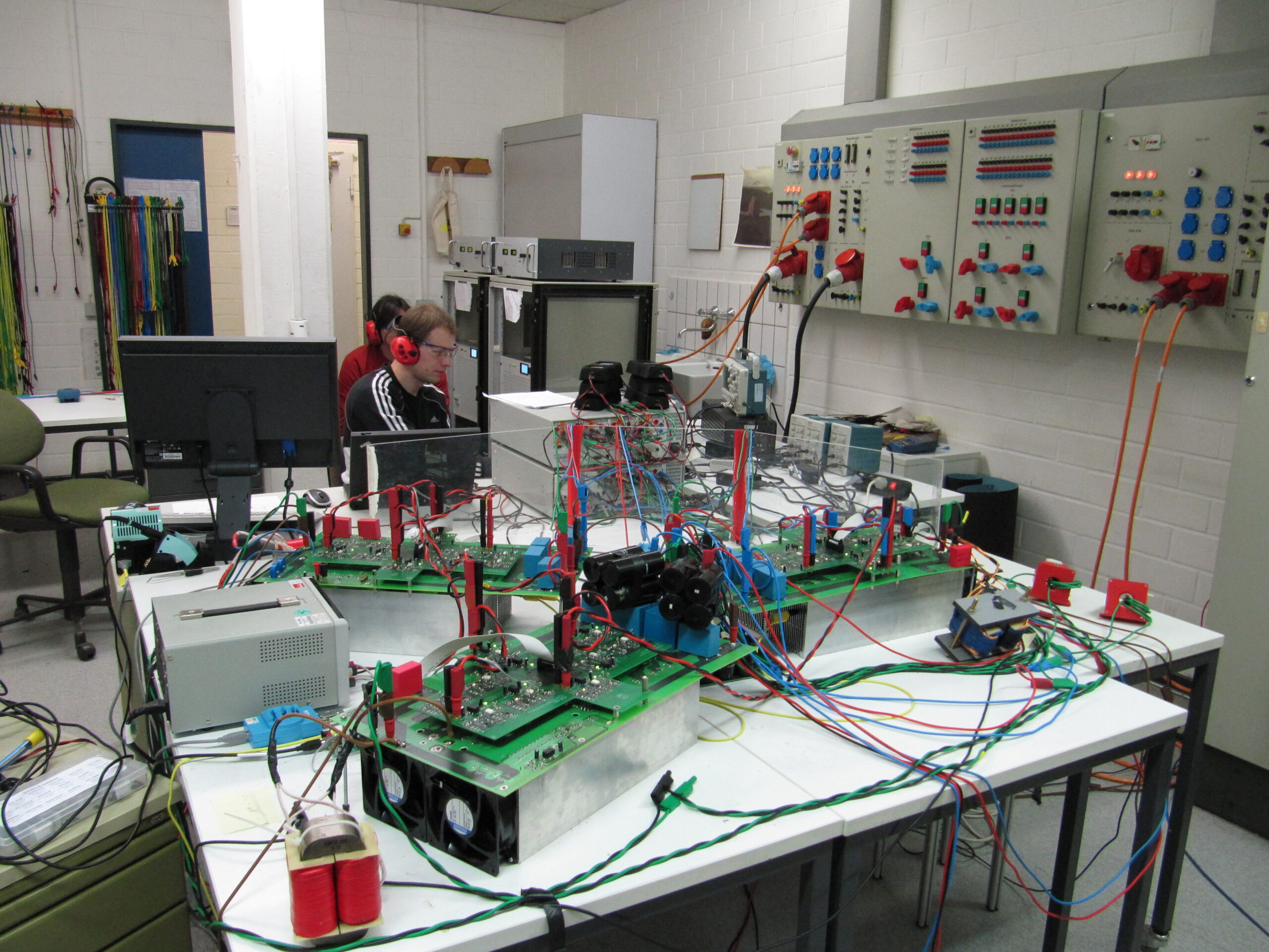
In the early 2010s the choice of specific topologies for a PV-inverter was challenging: SiC-MOSFETs were quite expensive, GaN-HEMTs not yet available and Si-MOSFETs had lots of different properties. So the question was: which topology is worth for a PV-inverter: pretty simple 2-level B6-inverter, 3-level NPC or BSNPC-inverter or maybe a 5-level inverter to reduce the size of the output-filters even more? So I designed a PCB with three different inverter-topologies to investigate the behaviour and performance of each of the three designs. It ended up in a total mess of wires spreaded of the tables in our lab, but I was able to achieve the desired results. Can you spot me in the picture?
Here is a picture of a single PCB:
3-phase PV-inverter with only 2 HF-switches?
During my masterthesis I had to investigate the chances to reduce the number of active high-frequency switches within a design of a PV-inverter. It was the year 2009 and semiconductors were much more expensive compared to todays devices. So Ned Mohan from the University of Minnesota published a very nice idea for a 3-phase rectifier – the Minnesota-Rectifier. As we can turn-around the basic idea of an active rectifier and create an inverter, this was my task here. I came up with a 3-phase bridge with six thyristors, that are much cheaper compared to MOSFETs. In front of this bridge I put a two-phase buck-converter that modulates not only a static DC-current, but a current with a huge 150Hz component.
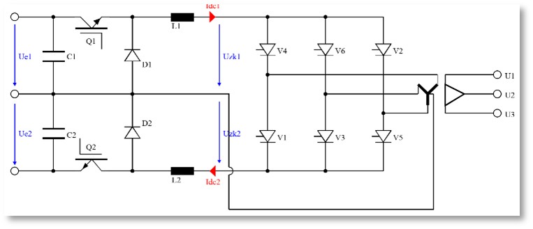
This 150Hz current was then distributed by the six thyristors to the three output phases. A transformer in a star-delta-configuration was then used to convert this 150Hz current-parts to a real 50Hz sine-wave:
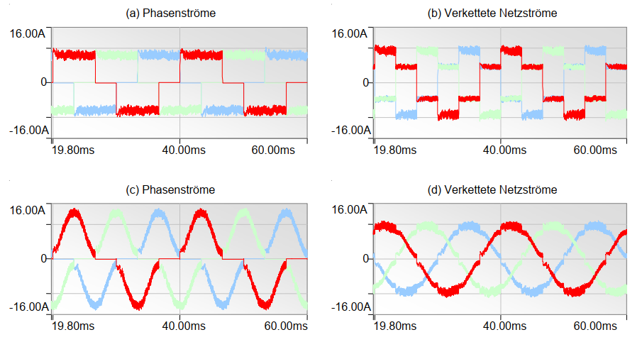
Here is the picture of the whole system with the two buck-converter inductors, the gate-driver-PCB and the main-PCB for distributing the current:
First contact with power-electronics
Right at the end of my studies in 2007 I started working on my first inverter-project. Fang Zheng Peng published a new type of inverter, mainly for automotive applications together with a fuel-cell:

The idea is to combine a current-source- and a voltage-source-inverter by using a cross-legged inductor-capacitor-network in front of the active switches. This allows controlled short-circuits of the semiconductor-bridge to charge the input-inductors and to boost the input voltage. But its also possible to use the bridge as a regular B6-bridge so that the input-voltage can be stepped down – pretty nice.
After some simulations I designed a control-system for our rapid-prototyping system to control all important parameters of my planned inverter-system:

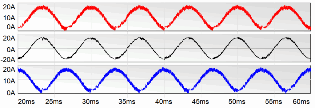
After around two weeks I finished the work on the PCB and was able to construct my very first inverter – and my very first PCB at the same time:
In the end the system had some problems regarding overvoltages on the input but overall I was pretty satisfied with my measured results (on the right) compared to the simulation (on the left):

Scientific hardware and software engineering
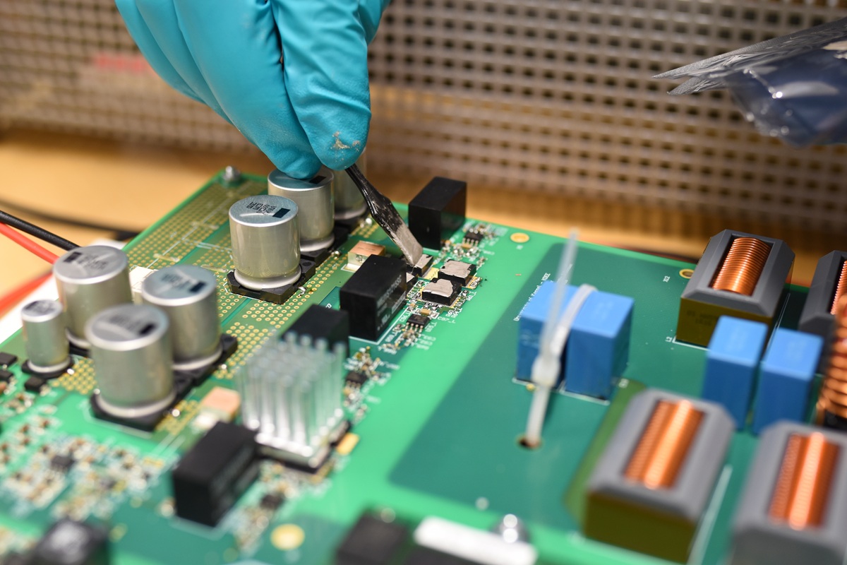
In the last years I was not within new research projects in full-time, but spent some time on developing smaller scientific instruments for measurement-purposes or for controlling laboratory equipment. One of my recent projects was to develop a pulse-generator for controlling high-speed semiconductors like SiC or GaN:
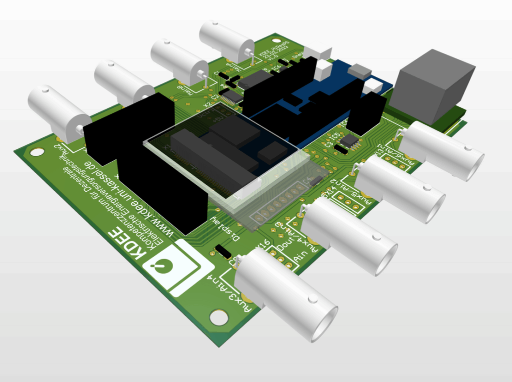
This device is able to output 8 control-signals with variable output-voltages with a timing-resolution of 10ns. Most of the time this is faster than the general jitter of the gate-drivers. This allows a perfect timing of turn-on- and turn-off-events of the semiconductors to test the devices.
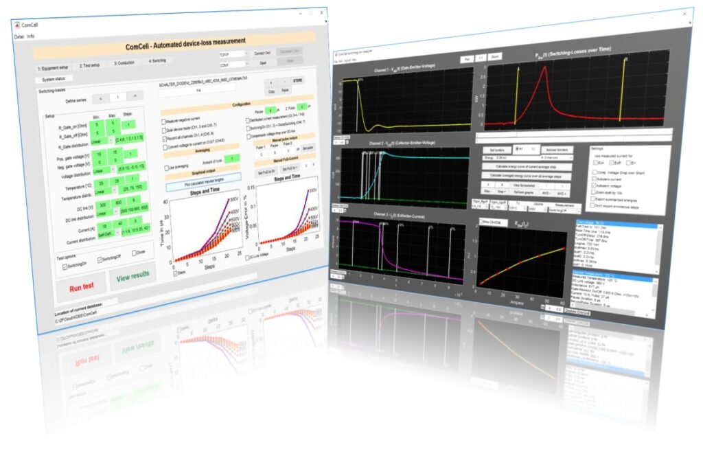
Since 2011 I’m working from time to time on a software to measure semiconductor-losses. This software is a small side-project that helps companies and my collegues to record important information about the switching-behaviour of a semiconductor like MOSFETs or IGBTs. Most of the time these devices are not operated at voltages, temperatures or currents that are within the datasheet and interpolating the available curves often does not lead to the expected behaviour – especially when the gate-driver and gate-resistor has different values compared to the manual:
That was a short trip to power electronics and the world of my University – at least some parts of it. If you like more information about our department, have a look at our website or have a look in our recent report, that can be downloaded as PDF here: LE Report